A blog about homebrew projects for Ham Radio. I cover aerials, test equipment, transmitters, both QRP and QRO, receivers and transceivers. The emphasis is on design and building. Generally I have boards and parts available at a modest cost. If you need more details, like a board layout, or any questions please ask. I'm more than happy to help.
Friday, 24 April 2020
NanoVNA Test Fixture - Details
Here is a picture of the fixture I am using. I had allowed for several fixture styles. At present I am using two of the fixtures, both single sided. The unused fixtures are double sided but I may never get around to trying them. The results to date suggest single sided is more than adequate.
The 50 ohm chip resistor fixture is shown on the top right hand corner. A tricky soldering job since one pad is underneath, and the other wraps around. Clearly too much solder but the OSL calibration process is hopefully negating the additional stray capacitance that blob is contributing to the measurements. Not obvious is the manual removal of the ground trace that runs under the chip resistor by scratching it off.
To calibrate the fixture I use the chip resistor version. As shown it is open circuit. I use a piece of foil squashed onto the SMA pins with my thumb as the short. The piece of foil is used to connect the pad adjacent to the ground side of the 50 ohm resistor to the untinned areas as the load calibration.
I then use the same calibration settings for both fixtures. Using the calibration for the chip resistor version with the non-chip resistor version has proven to be acceptable.
To use the same fixture without the resistor I sweat soldered a piece of tinned copper foil as shown. The SMD then is placed where the pad for the chip resistor was used to connect to the center pin of the SMA connector. That tiny chip inductor is I think 0201. It was the smallest physical and electrical value I have tested to date, with good results. But more on that later.
I hold the test device in place by clamping it with a wooden clothes peg. Sometimes I use a piece of bare fiberglass, or other benign material like the fingernail on my thumb, and I have found no material difference in readings by doing this.
Experience with this fixture suggest I should have made the pad slightly larger to more easily accommodate some of the SMD inductors just larger than 1206 size parts. And maybe shaped the ground pad to be closer to make placing the 0201 parts a little easier.
Thursday, 23 April 2020
NanaVNA - Test fixture for measuring passives
Recently I've been exploring what the NanoVNA can do. It really is an impressive piece of test equipment for such a small sum. There has been lots of discussion about measuring passives at HF but I was troubled by the lack of evidence that some commentators had actually done what they advocated. Just like fake Chinese transistors, too many online experts write on the basis of what they have read, not what they have done.
And there was very little online information I could find about using the NanoVNA to measure very small values of passive components. What information I could find was at times inconsistent. So I set out to discover for myself what worked. Over the next few weeks I'll post what I found.
But first the starting point has to be the text fixture. I had a PCB house fabricate a few boards so I could experiment. A variety of single and doubled sided layouts were contemplated, some would use a 50ohm chip resistor in series with the passive being tested, some would simply place the passive component across the SMA.
My biggest challenge was presenting the test results. Taking a picture of the screen was impossible given the screen reflections. "nanoVNA partner" is a small download and worked well on both XP and Windows 10. I recommend it.
As far as using the NanoVNA, at least one published paper would appear to advocate a different approach to what I found. Could it be the NanoVNA was better than the equipment used in that published paper?
Saturday, 23 November 2019
40m Direct Conversion Receiver - modification for low signal levels
Pleasing to see the level of interest this project has generated. There has been an on-air problem which does not show up in bench testing and the explanation and correction for that follows.
Issue:
The AGC does not compensate for very weak signals. This is only noticed in very low noise environments and requires manual adjustment of the volume control to hear these weak signals.
Explanation:
The generation of the negative rail for the audio stages is injecting ripple onto the plus and minus 12V rails. This ripple is inaudible but the decoupling is not sufficient to prevents the AGC from believing it is a valid audio level. Weak received signals reaching the AGC which are lower than the ripple are not benefiting from the AGC increasing the audio gain to compensate.
The issue was overlooked on the bench when weak signal testing because the volume control had been manually adjusted.
Correction:
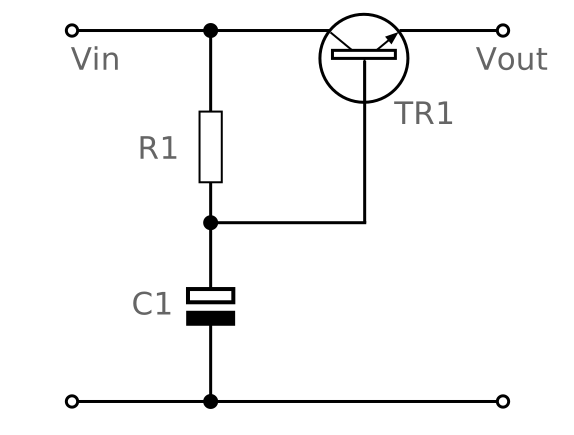
The decoupling of the 12volt rails by the 68ohm and 22uF capacitor is insufficient. To reduce the voltage drop that would occur if R was increased a capacitor multiplier using a transistor is used. The 68 ohm resistor is changed to several k and this RC connection is made to the base of a transistor.
See sites like https://www.electronics-notes.com/articles/analogue_circuits/transistor/capacitance-multiplier-circuit.php for an explanation of how this works.

Note that a npn transistor is used for the plus 12v rail and a pnp transistor for the negative 12v rail.
http://electronics-diy.com/electronic_schematic.php?id=486 shows how the emitter and collector connections are reversed for the pnp transistor on the negative rail.
Outcome:
The AGC action now includes very weak signals.
Issue:
The AGC does not compensate for very weak signals. This is only noticed in very low noise environments and requires manual adjustment of the volume control to hear these weak signals.
Explanation:
The generation of the negative rail for the audio stages is injecting ripple onto the plus and minus 12V rails. This ripple is inaudible but the decoupling is not sufficient to prevents the AGC from believing it is a valid audio level. Weak received signals reaching the AGC which are lower than the ripple are not benefiting from the AGC increasing the audio gain to compensate.
The issue was overlooked on the bench when weak signal testing because the volume control had been manually adjusted.
Correction:
The decoupling of the 12volt rails by the 68ohm and 22uF capacitor is insufficient. To reduce the voltage drop that would occur if R was increased a capacitor multiplier using a transistor is used. The 68 ohm resistor is changed to several k and this RC connection is made to the base of a transistor.
See sites like https://www.electronics-notes.com/articles/analogue_circuits/transistor/capacitance-multiplier-circuit.php for an explanation of how this works.
Note that a npn transistor is used for the plus 12v rail and a pnp transistor for the negative 12v rail.
http://electronics-diy.com/electronic_schematic.php?id=486 shows how the emitter and collector connections are reversed for the pnp transistor on the negative rail.
Outcome:
The AGC action now includes very weak signals.
Subscribe to:
Posts (Atom)
