It's been about 4 weeks now and some observations of the impact pulse conditioning has had on internal resistance and perhaps battery capacity are warranted. More importantly, the need for a more rigorous approach has become apparent.
Over that last 4 weeks the measured internal resistance has fallen from 264 milli-ohms to 175 milli-ohms. While the reduction in the internal resistance tapered off after about 10 days, there is some support for the battery's capacity having increased as well. At the start I was recharging the battery after 3 days on the pulse conditioner. Now it runs for 5 to 6 days before I have to recharge the battery.
So my initial observations are that the pulse conditioner is beneficial. However, there are several issues with the approach and the results cannot be construed as anything other than weak support for pulse conditioners.
The biggest drawback to the approach is the lack of a control battery. With a second battery I could cycle one on the pulse conditioner whilst the other was cycled on a static load. If the static load battery showed little, or no improvement, in internal resistance then there would be much stronger support for the pulse conditioning approach.
Another drawback stems from the lack of automation. I still have to manually changeover the battery at each step of the pulse, charge, measure cycle. So the time between measurements is not constant and the level of charge and discharge varies from one cycle to the next. I clearly need to automate the cycle and let it run unattended.
The final obvious shortcoming is temperature. We are moving towards summer and the average ambient temperatures have increased over the last month. The temperature change could be influencing the results either directly via battery chemistry somehow, or indirectly by it's impact on the voltage regulator which serves at the voltage reference for the D2A conversion. A temperature controlled testing environment would be useful to remove another source of potential error but that is beyond my reach at present.
The biggest obstacle to the full automation with the W1209 board is the need for an additional two digital outputs. I have considered two approaches. The first is using the + and - keys as both inputs and outputs. That would require some careful soldering to insert a resistor, say 2k, in series with each switch. The second approach is a 4017 counter clocked by the pin driving the relay. Then each of the decoded outputs for 1-3 from the 4017 driving a relay to perform each step of the pulse charge measure cycle.
I'm leaning towards the first approach since I don't know if I have a 4017 in the drawer and the first approach avoids any ambiguity over which step the cycle is in.
Thursday, 5 October 2017
Tuesday, 12 September 2017
Lead Acid Batteries - Measurement of Internal Resistance - V3 of Code
After hours running various tests to determine when the voltage
samples should be taken I concluded there was no right answer. Mind you,
the sweet joy of using Forth to do this via the serial port was a
reward in itself. ( Timing loops could be tested interactively, results
displayed on the terminal window, etc etc. )
I settled on a longer delay before sampling the loaded voltage, or Vend in the code, then a short delay before sampling the unloaded voltage, or Vbeg in the code. Because of the way the voltage depresses over time, then recovers, I doubt there is a right way to do this. But my training in Statistical Process Control and Gauge Capability steered me in this direction.
I now have a testing method that gives me repeatable readings provided each test is run hours apart. So while the calculated internal resistance might not be the value according to some standard it should allow me to discern if my pulse conditioning circuit has any impact over time on the internal resistance.
Over the next few weeks I'll run my trials and see what happens.
Monday, 11 September 2017
Lead acid batteries - Measurement of internal resistance - x4 resolution mod
The initial project used a voltage divider to reduce the measured voltage down to less than 5V. This means the voltage resolution is about 20mV which means the internal resistance measurement for 1 amp of current is 0.020 ohms.
Instead of dividing by 4 with a resistor string, what if we subtracted 10V from the voltage to be measured? This would give us a voltage resolution of about 5mV with an internal resistance measurement for 1 amp of current is 0.005 ohms. This seems like a worthwhile improvement and can be easily achieved.
I had never played with a voltage subtracter before but it proved to work first time. Reaching into the junk box I pulled out a NE5532 dual op amp. I had no reason to chose this device over any other except I had hundreds I had recovered from a couple of boards. A few resistors and it was done.
While I used a NE5532 and 2.4k resistors I don't think there is anything critical about this. Just about any op amp will probably work and the resistors could be anything between perhaps 1k and 100k. As long as they are all the same value.

As before I'll post the updated code over on Hackaday. While this is not yet the complete measurement tool I wanted it will allow me to make some measurements on the impact, if any, pulse conditioning has on internal resistance.
Sunday, 13 August 2017
Lead acid batteries - Measurement of internal resistance - Code
While working on a small hardware modification to improve the resolution of measurements it occurred to me that displaying an internal resistance of 0.2 ohms as 200 was easier to read than 2. I updated the code over on Hackaday
Debugging a change like this is so easy with Forth, especially when a simple x100 instruction fails because the 16 bit integer maths overflows.
Regards
Richard
ps the hardware mod worked a treat giving a fourfold improvement in resolution. I'll describe it shortly once I've finished the soldering. It might even mean that no modifications to the board are required!
Saturday, 12 August 2017
Lead acid batteries - Measurement of internal resistance - Schematic
Once you have modified the W1209 board here is the schematic for the overall project as it stands today.

Regards
Richard VK6TT

Regards
Richard VK6TT
Friday, 11 August 2017
Lead acid batteries - Measurement of internal resistance
Hams, listen up. With our short arm deep pockets mentality this is going to really appeal to you. This project takes a cheap assembly, $2 delivered, from China and turns it into a test fixture for measuring the internal resistance of small lead acid batteries.The project as it stands works very well. However, I've already thought of ways to improve it which I will incorporate in due course and report on.
There were two motivating reasons for this project. The first, and a long standing one, was to measure the internal resistance of lead acid batteries to see if some of the rejuvenate, repair or restore ideas I had come across had any objective merit. As a ham I have plenty of small lead acid batteries which I only require occasionally. I periodically float charge them and occasionally I have had to dispose of one via the recycling depot after cells have gone open or short circuit. Recently I began playing with a pulse conditioning circuit and initial measurements of internal resistance suggested there was some lowering of the internal resistance. But manually setting up a test jig and then remembering to take measurements has been a problem for someone so easily distracted.
So I was looking for a way to automate the entire measurement, conditioning and charging process to firmly establish if there was any benefit in pulse conditioning these batteries. Then I stumbled across the project at eForth for cheap STM8S gadgets • Hackaday.io which is one of the most exciting ideas I have seen in recent times. The thought of taking a $2 board, replacing the firmware, and doing something entirely different with it just thrills me. The more I use these gadgets the more ham applications I see.
This project uses the W1209 thermostat board, readily available for under $2. Delivered. Hams, listen up. What I did was make a few small modification to the board:
At present my board works as follows:
My longer term goal is a test fixture that repeats daily a charge of the battery, measure the internal resistance, then applies the pulse conditioning until it is time to start the cycle over again. Then once every 8 weeks I can either dump the data back to the PC by reading the eeprom, or read the data via the display for whatever run I chose.
Over a series of posts I will cover the initial Forth code and subsequent improvements, the circuit for the 1A constant current load, how everything is wired up and eventually the further modifications to improve the resolution.
In the meantime here is what you need to do. Firstly, read the hackaday link above for background information. I really like the programmable power supply. I can see several of those going onto my workbench in due course. The team behind this Forth project need a big thank you for doing such a great job.
If you decide to give Forth a try, and I strongly encourage you to do so, your shopping list is:
I will post working copies of my firmware if you simply want to flash the board and not learn Forth. And if all you want is a pre-programmed modified board then you best contact me.

There were two motivating reasons for this project. The first, and a long standing one, was to measure the internal resistance of lead acid batteries to see if some of the rejuvenate, repair or restore ideas I had come across had any objective merit. As a ham I have plenty of small lead acid batteries which I only require occasionally. I periodically float charge them and occasionally I have had to dispose of one via the recycling depot after cells have gone open or short circuit. Recently I began playing with a pulse conditioning circuit and initial measurements of internal resistance suggested there was some lowering of the internal resistance. But manually setting up a test jig and then remembering to take measurements has been a problem for someone so easily distracted.
So I was looking for a way to automate the entire measurement, conditioning and charging process to firmly establish if there was any benefit in pulse conditioning these batteries. Then I stumbled across the project at eForth for cheap STM8S gadgets • Hackaday.io which is one of the most exciting ideas I have seen in recent times. The thought of taking a $2 board, replacing the firmware, and doing something entirely different with it just thrills me. The more I use these gadgets the more ham applications I see.
This project uses the W1209 thermostat board, readily available for under $2. Delivered. Hams, listen up. What I did was make a few small modification to the board:
- remove the 20k smd resistor next to the sensor connector,
- throw the sensor in the junk box,
- add a 10k resistor across the sensor connector (underneath if a smd resistor or remove the connector if using a through hole resistor)
- add a 30k resistor (or two 15k resistors in series) from the upper terminal of the sensor connector to the +12v rail.
At present my board works as follows:
- after connection to the battery I hit the "+" key to run the measurement routine. It takes about 1 second and in that time it reads the battery voltage 32 times, summing the result, activates the relay which increase the current drawn by 1 amp and takes a further 32 measurements of the battery voltage summing those results, releases the relay then saves these two sums into eeprom
- I then hit the "set" key and the display shows me the average of the open circuit voltage, the loaded battery voltage, and the calculated internal resistance.
- If I hit the "-" key the run counter is reset to zero.
My longer term goal is a test fixture that repeats daily a charge of the battery, measure the internal resistance, then applies the pulse conditioning until it is time to start the cycle over again. Then once every 8 weeks I can either dump the data back to the PC by reading the eeprom, or read the data via the display for whatever run I chose.
Over a series of posts I will cover the initial Forth code and subsequent improvements, the circuit for the 1A constant current load, how everything is wired up and eventually the further modifications to improve the resolution.
In the meantime here is what you need to do. Firstly, read the hackaday link above for background information. I really like the programmable power supply. I can see several of those going onto my workbench in due course. The team behind this Forth project need a big thank you for doing such a great job.
If you decide to give Forth a try, and I strongly encourage you to do so, your shopping list is:
- a few of the W1209 modules, pictured below,
- the programming dongle,
- and a serial interface (USB dongle or MAX232 based device) if you don't already have one.
I will post working copies of my firmware if you simply want to flash the board and not learn Forth. And if all you want is a pre-programmed modified board then you best contact me.

Tuesday, 27 June 2017
Satellite Tuner Board becomes a 800MHZ - 1600MHz Signal Generator
I've been so busy on non Ham activities that I haven't had a chance to pursue my Ham projects. As a stop-gap measure here is something I recently finished. While it doesn't neatly fit the goals of my blog to be easily repeatable by the reader it will hopefully inspire you to attempt something similar. If you have one of these satellite receiver boards then I can provide further details and code to help.
A while back a generous Ham, Fritz, was giving away some satellite tuner boards at the NCRG Hamfest. The board had a nice TXCO but on closer inspection it also had some nice PLL chips (Si4133) and mmic amplifiers. So I downloaded the relevant datasheets and ruminated on what it could be used for. My ultimate goal is to use one of these to generate a WSPR transmission on 1296MHZ. But you have to crawl before you can walk!
Before modification the PLL section of the board looked like this:

After removing the superfluous controller chip from elsewhere on the board and cutting the board to fit into an enclosure it became a matter of delicately soldering some thin wires onto relevant via's. These wires then went to a new control board I made.
It transpires that my version of the chip did not have the IF Out function. Which meant I couldn't use it for 70cms or 2m. However, each PLL chip had two PLL's and I found I could cover 800 MHz to 1600 MHz in four overlapping ranges, with steps down to 10kHz. The only drawback was I couldn't load the frequencies fast enough to also make this work as a micro-controller based frequency sweeper. Each frequency change took around 50ms to achieve.
In due course I hope to take some photographs of the noise sidebands as the step size, or phase detector frequency, changes. This should illustrate why the largest possible step size should be used if you are interested in signal purity.
The chip can be purchased for around A$10 (US$7) in a TSSOP package which would be easier to work with than the ones I had on the tuner board. Which is why I didn't remove them but used them in-situ. If you would be interested in building one from scratch let me know. I think a signal generator that covered 2m, 70cm and 23cm would be a great project with a cost around A$50 (US$35).
While kits exist that generate frequencies like the ones this project does, there is enormous satisfaction in re-purposing something that was meant to be scrapped.
Regards
Richard VK6TT
Wednesday, 17 May 2017
Etching Tank
I've been busy on non-ham activities the last few weeks so I haven't progressed many projects. I'm re-organising the workshop and trying to throw out some equipment surplus to requirements. My wife calls it junk!
I had a few SCSI tape drives lying around and as I opened one up to recover the controller board it occurred to me I could make a tank agitator for etching. In the past I had used an aquarium bubbler with an air stone. I stopped using this because it generated a plume of etchant that stained nearby objects. I moved on to putting the pcb in a zip lock back and manually rocking it while it sat in a dish.
This works well but if I could automate the rocking and heat it at the same time things would be better. I'm blessed with a working stove and hot plates in the workshop, but don't tell the wife or I might be expected to move into the workshop for good.
So there when I opened the SCSI drive was a great big cog used to load the tape. It took all of 5 minutes to work out there was a lug underneath the cog I had to chop off so it could rotate continuously and wire up a plug pack to the motor. A few more minutes to work out how to attach the rotating cog to the etchant bath and I was done. I used a bolt onto a pop stick, or small piece of wood found in frozen ice sweets, and a piece of string from the wood to a peg on the dish.
With the hotplate turned on and the motor running things went smoothly. The only issue is the dish tends to walk around the surface of the hot plate. I'm going to fix that by running the cord over an arm and pulley perhaps 50cm above the etchant tank. That way the lifting on the tank will be vertical instead of including a side to side motion as well.
The current arrangement looks like this before I make the arm and pulley:

A very temporary proof of concept. Which just goes to show that one man's junk can contain his treasure.
Regards
Richard VK6TT
Friday, 5 May 2017
Heatsink Fan Temperature Switch
As I was pondering the next step with my bag of 2SC5707 transistors the problem of heat-sinking occurred to me. An elegant solution would be to mount the transistors to the PCB but the cooling is awkward. Then I remembered how effective forced air cooling is and remembered I hadn't shared this with readers before.
I put most commercial class VHF FM transceivers way ahead of ham gear when it comes to selectivity and immunity from pagers. The only drawback I have ever noticed was with regard to transmitting duty cycle. Generally, the commercial transceiver was never intended for long overs and the heat-sinking reflects this. Fine for repeater use but if you have a long over on simplex things get hot. Sometimes very hot!
Here is a simple project that really protects that radio. First, the results of before and after measurement of heat-sink temperatures are shown below on a Philips PRM80 transmitting 25 watts into a dummy load:

It is true that many transmissions do not last 3 minutes or longer. However, a high SWR at the radio will increase the heat dissipated by the final transistor. I generally only check my antenna when I suspect it needs to be checked. So I could be transmitting for some time before any problem is detected. And while I have never sat on the microphone I am sure we have all heard someone driving around with the transmitter keyed up for extended periods.
I consider this a worthwhile addition to any PMR type radio. From the circuit below you will see that when the output of the temperature sensor reaches a set point the fan is turned on. Once the temperature falls the fan turns off.
 I made mine on a small 0.8mm thick piece of PCB so that the surface mount LM61 could be mounted in a slot in the board to make contact with the heat-sink when the pcb was bolted to the heat-sink.
I'm going to use the same circuit on a forthcoming experimental HF amplifier using all of my remaining 2SC5707's. One last hurrah for them or a successful 15 watt linear amplifier for the lower HF bands.
Regards
Richard VK6TT
I put most commercial class VHF FM transceivers way ahead of ham gear when it comes to selectivity and immunity from pagers. The only drawback I have ever noticed was with regard to transmitting duty cycle. Generally, the commercial transceiver was never intended for long overs and the heat-sinking reflects this. Fine for repeater use but if you have a long over on simplex things get hot. Sometimes very hot!
Here is a simple project that really protects that radio. First, the results of before and after measurement of heat-sink temperatures are shown below on a Philips PRM80 transmitting 25 watts into a dummy load:

It is true that many transmissions do not last 3 minutes or longer. However, a high SWR at the radio will increase the heat dissipated by the final transistor. I generally only check my antenna when I suspect it needs to be checked. So I could be transmitting for some time before any problem is detected. And while I have never sat on the microphone I am sure we have all heard someone driving around with the transmitter keyed up for extended periods.
I consider this a worthwhile addition to any PMR type radio. From the circuit below you will see that when the output of the temperature sensor reaches a set point the fan is turned on. Once the temperature falls the fan turns off.

I'm going to use the same circuit on a forthcoming experimental HF amplifier using all of my remaining 2SC5707's. One last hurrah for them or a successful 15 watt linear amplifier for the lower HF bands.
Regards
Richard VK6TT
Friday, 28 April 2017
Test Equipment Tip for Initial Testing of Transmitter Amplifiers
While many of us start out building transmitter stages and tuning for maximum output, we should quickly learn that over-driving a transmitter stage must be avoided. Even a slightly over driven amplifier stage generates significant harmonics and distortion products. So here is a quick tip on using the oscilloscope to check for the presence of a transmitter stage being over-driven.
A 10MHz analogue oscilloscope will be fine for looking at HF signals since we are going to measure relative voltages. I am unsure if a low bandwidth digital CRO will work.
Connect your oscilloscope to the collector or drain of the active device. With no drive and the oscilloscope set to AC coupling ensure the horizontal trace is on the centre graticule. The time-base setting is not critical so I use something that gives me a band across the screen with drive applied rather than the actual waveform. Try 1ms per division and adjust to suit your preference.
Now apply perhaps 10% of the drive you expect to use when the amplifier is in operation. Adjust the trace so it sits between say the second graticule above the centre line and the second graticule below the centre line. As you increase the drive you should see the trace touch the third graticule above and below the centre line at the same time.
Adjust the vertical amplifier gain to reduce the signal size on the screen then increases the drive again. Again, you should see the trace touch the third graticule above and below the centre line at the same time. Keep repeating this until you notice that one of the third graticule's above or below the centre is being touched before the other is being touched.
At this point the amplifier is no longer linear. If you have a fast oscilloscope you can increase the time-base speed to observe a few cycles of the waveform. You will notice that when non-linear the waveform peaks that were last to hit the third graticule will be distorted.
You can back off the drive until both the positive and negative peaks are moving in unison, which I find easier to discern with a slow timebase setting rather than a few cycles being displayed on the screen. That is the limit for linear operation of the stage.
Spectrum analysers and other nice test gear allow you to measure how non-linear your transmitter is. But isn't it easier just to avoid over-driving the transmitter to begin with? Hopefully this tip helps you avoid over-driving your transmitter stage giving you a nice clean signal when you finally go on air.
Regards
Richard VK6TT
Tuesday, 25 April 2017
250mW Class A Amplifier with 2SC5707
Further to my recent posts on using the 2SC5707 of unknown origin I finally got around to some more testing. I calculated the component values for a 250mW Class A amp and after etching a circuit board built the amplifier for testing. Overall, the results were pleasing and justify further experimentation.
Referring to my bible, "Solid State Design" by Hayward and DeMaw, I expected a gain of 17dB from the circuit below:

I achieved this 17dB of gain at 10MHz. However, the gain had fallen by 4dB at 20MHz so at present I will limit my use of this transistor to 14MHz and lower.
My clip on heatsink was a 15mm x 15mm piece of circuit board, held on with a wooden clothes peg. Worked extremely well for testing but I have a more permanent solution in mind which I will post about shortly.
Overall a nice little amplifier and I will box it up for use on the workbench to increase the drive from my signal generator as required. But ironical that it will be a 15c transistor between two expensive BNC connectors.
With 8 transistors left I will really push them in the next experiment to see if there is any smoke in them!
Thursday, 30 March 2017
Testing my Noise Source and 2m Band Pass Filter - update
Yesterday I caught up with Jack, VK6KDX's, and enjoy the pleasure of chatting about his projects while drinking his coffee. A great way to spend a few hours.
One of the activities we pursued was looking at the output spectrum of noise sources on some test gear Jack owns. Jack demonstrated his noise source and it works very well for testing 23cm filters. We then had a look at my noise source on the spectrum analyser. It had peaks and looked horrible. It occurred to me this morning that the reason for that was most likely stray RF being coupled into the noise source and being amplified by the mmic chain. I still haven't put my noise source into a metal box and the power supply decoupling could be greatly improved.
Despite the shortcomings of the test set-up it did allow me to see the 2m Band Pass Filter in action. A small shoulder on the left of the response curve could be either stray RF coupling or a result of this being a no-tune filter. But I'm really happy with both the noise source and the filter. Especially the filter. It's always pleasing when you build something that confirms your measurement technique for the inductors is really good. No trim-caps, no squeezing or expanding coils. Measure, design and build. Worked first time with no tweaking.

The spectrum analyser was set to 146MHz, 20Mhz per division. We didn't check or adjust for any drift in the spectrum analyser itself. As expected the response falls off faster on the high side. If you haven't read how I measure nH inductors then check out the post http://vk6tt.blogspot.com/2017/01/measuring-small-inductors.html.
Regards
Richard VK6TT
Thursday, 23 March 2017
Testing my Noise Source and 2m Band Pass Filter
Well it turns out I couldn't readily find anyone with the test gear to look at my homebrew noise source. I will keep asking around but in the meantime I thought I'd see if it could be used to determine the response of the 2m bandpass filter I described in this post.
The first thing I did was look at the noise source output across the spectrum in 10MHz bites with my spectrum analyser. It wasn't flat. The was about +/- 2dB from 10MHz to 1GHz. So any measurements would have to be on a before and after basis.
So I put the 2m filter between the noise source and the spectrum analyser and used the peak hold function as a surrogate for an average over time. I measured the response every 10MHz from 85MHz to 205MHz. Then I removed the filter and measured the levels again. Subtracted the difference and I had a response curve.
Here then is the measured results against what was modelled:
 If you look closely the measured response is indicated by the 'dot' at each marker. Clearly something is not quite right. Somehow the filter has "gain" at 135MHz and 145MHz. That somehow is not possible. And the measurement at 125MHz looks odd.
I had previously measured the filter response into a good 50 ohm power meter and it was a very close match to what was modelled. Hence, the distortion in the measured results was due to either the spectrum analyser not being a true 50ohm resistive input or the patch leads were not 50 ohms. Either way it shows that the noise source can be used for measurement, but only when the test gear is not influencing the result.
Perhaps the reason for the +/- 2dB response a cross the spectrum is due to the spectrum analyser input impedance. Once I find another piece of test gear to measure the noise source on I will know more. In the meantime, I'm using the mythbusters approach and calling the noise source project finished.
Since this noise source costs peanuts I urge you to build one, or something similar, and comment on how it went.
Regards
Richard VK6TT
The first thing I did was look at the noise source output across the spectrum in 10MHz bites with my spectrum analyser. It wasn't flat. The was about +/- 2dB from 10MHz to 1GHz. So any measurements would have to be on a before and after basis.
So I put the 2m filter between the noise source and the spectrum analyser and used the peak hold function as a surrogate for an average over time. I measured the response every 10MHz from 85MHz to 205MHz. Then I removed the filter and measured the levels again. Subtracted the difference and I had a response curve.
Here then is the measured results against what was modelled:

I had previously measured the filter response into a good 50 ohm power meter and it was a very close match to what was modelled. Hence, the distortion in the measured results was due to either the spectrum analyser not being a true 50ohm resistive input or the patch leads were not 50 ohms. Either way it shows that the noise source can be used for measurement, but only when the test gear is not influencing the result.
Perhaps the reason for the +/- 2dB response a cross the spectrum is due to the spectrum analyser input impedance. Once I find another piece of test gear to measure the noise source on I will know more. In the meantime, I'm using the mythbusters approach and calling the noise source project finished.
Since this noise source costs peanuts I urge you to build one, or something similar, and comment on how it went.
Regards
Richard VK6TT
Tuesday, 14 February 2017
Noise Source Part 1 - Construction
I've heard of several local hams buying noise sources from China in recent days. I had read that they were based on this circuit found here and a quick look at the pictures in the listing supports this. I wondered how hard this could be?
I knew I had too many MAR03 mmics in the parts draw which I now never use. A quick Google and I came across an alternative approach here. So I quickly put a string of mmics into the pcb software and came up with a schematic and board as shown below:


I used whatever 1206 size inductors were in my parts bin for I1 to I4. I used a selection of values just in case this avoided some weird response in the output spectrum. One of the improvements I made was to put an attenuator on the output. It appears often overlooked but not all mmics have a good match to 50 ohms on the output port. The ERA5, used in the first example, is very good and would only see a small improvement with an attenuator. But since I didn't have one to hand I used a small amount of attenuation to bring this project closer to a 50 ohm output impedance.
I went up to the workshop and etching a board as follows:
I print an outline layer of the pcb and cut a piece of Cricut vinyl to suit.

I then remove the backing from the vinyl and print the layer onto it. It helps when you print the outline if you put a crease on the bottom corner of the paper to mark which way it goes back into the laser printer.

Then I iron this onto my pcb. Normally large black areas give me trouble because laser printers struggle to print dense large areas. So I tried something different today. I had just received some eBay sheets of gold foil transfer. In theory you put the grey side onto the toner and apply heat and pressure. It looks a bit rough but let's see what happens after etching.

I pulled the board out of the bubble bath and my initial concern was the patches of toner showing. Perhaps the toner density would prove too light and some etching of the groundplane areas would occur?

Only one way to know. I wiped the board with acetone to get this:

Apart from a few minor blemishes, particularly where the insulation tape crept up towards some tracks, everything looked good. The gold foil is definitely part of my standard procedure from know on.
So I fixed the minor issues and build this. Initial testing shows it works but I need to visit someone with better test gear than mine to verify this. As always if you need more details please ask.
I will report back soon on the testing.
Regards
Richard VK6TT
Friday, 10 February 2017
Quadrature Networks for Phasing Transceivers - Measurement Matters
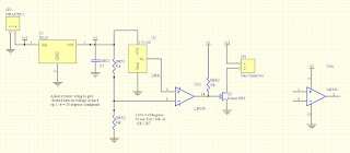
I previously blogged, here, how I used a Wheatstone Bridge to match resistors and was surprised by how easy it turned out to be. The reason for matching resistors was to build a quadrature network for audio phase shifting. You need sets of matched resistors to ensure the op amp gain of each stage is unity.
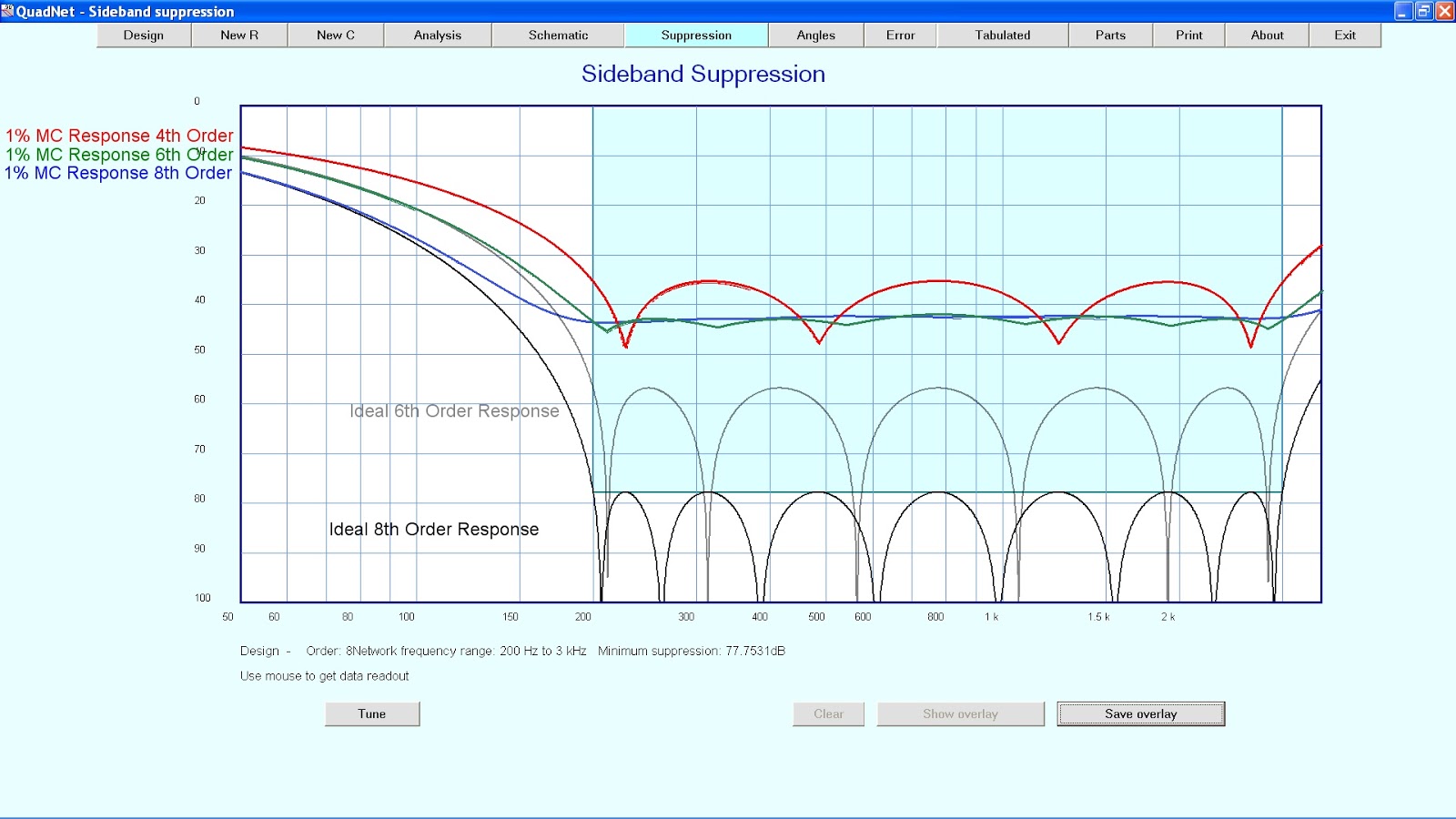
Today I was contemplating how complex does this network need to be. I fired up Quadnet, from Tonne Software, and examined this issue. It turns out that if you are just going to accept that the best tolerance you can achieve is 1% then there is little point in using an 8th order filter. The monte carlo shows that the worst result for the 6th and 8th order filters is largely identical.

While 43db or so of sideband suoppression is a good starting point if you have the worst case outcome, the improvement with tighter tolerances is considerable. You might get closer to 55db of sideband suppression with a 6th order filter, or 77db with an 8th order filter.
I like the way this software allows you to measure a capacitor and then use that value to determine the required resistor values. With a bunch of measured capacitors you could tweak the placement of these and the resulting resistor values to get the best result.
More thought is needed before I decide on a course of action. However, it does illustrate the point that garbage in garbage out applies. Since I strive to get the best out of anything I do I will have to think about calibrating my digital LC meter now.
Regards
Richard VK6TT
Today I was contemplating how complex does this network need to be. I fired up Quadnet, from Tonne Software, and examined this issue. It turns out that if you are just going to accept that the best tolerance you can achieve is 1% then there is little point in using an 8th order filter. The monte carlo shows that the worst result for the 6th and 8th order filters is largely identical.
While 43db or so of sideband suoppression is a good starting point if you have the worst case outcome, the improvement with tighter tolerances is considerable. You might get closer to 55db of sideband suppression with a 6th order filter, or 77db with an 8th order filter.
I like the way this software allows you to measure a capacitor and then use that value to determine the required resistor values. With a bunch of measured capacitors you could tweak the placement of these and the resulting resistor values to get the best result.
More thought is needed before I decide on a course of action. However, it does illustrate the point that garbage in garbage out applies. Since I strive to get the best out of anything I do I will have to think about calibrating my digital LC meter now.
Regards
Richard VK6TT
Monday, 6 February 2017
AD8307 Power Meter - Mk2

I was never happy with the meter being driven off-scale until the pot had been adjusted. This time, I used a small micro to generate the reference voltage with a D2A based on a R2R ladder network. I wrote some code so that at power up, a form of reset, the micro started increasing the reference voltage until a threshold was reached. Then it simply stopped. Now I had automated this part of the process my Q measurement procedure became:
- find the peak response,
- flick over to meter to the x10 setting,
- turn the power off and back on, thereby resetting the micro and generating a useful reference voltage
- then to check the Q I look for a response 30dB less than the peak shown on the meter.
This made it even easier to measure -3db frequencies when looking at inductor Q, crystal parameters or trying to get that last 0.1dB improvement when adjusting filters.
Since the R2R network is only 4 bits, the reference voltage to the differential amplifier has 16 steps and I chose the upper resistor on the network to compress those 16 steps into the range needed.

Naturally you're welcome to the code and board design. Get in touch and I will shoot it across. I still haven't worked out how to make it available from my blog.
Regards
Richard VK6TT
Thursday, 2 February 2017
AD8307 Power Meter
Here is what my current AD8307 power meter looks like. I built this into a "box within a box" to enhance shielding. Inside the case is the battery, a lipo cell, and it's charging regulator. When I want to charge it I plug it into a 12V power supply. The remaining RF circuitry is built into a shielded compartment at the rear of the front panel bnc. It's basically 99% air inside the case!


I use a pretty much standard circuit for the AD8307. I think it was Wes Hayward, W7ZOI
and Bob Larkin, K7PUA that first promulgated this in QST, June 2001. I dispensed with offset and calibration adjustments since I was quite happy with AD8307 as it stands.
However, it occurred to me one day that being able to zoom into the response would be really handy when looking for the 3dB down point when trying to measure inductor Q with my fixture, here. While it would be easy to add a dc amplifier, the input signal would have to be adjusted so that the amplifier did not saturate. My modification was to add a differential amplifier based on an op amp so that rather than adjusting the RF levels, one could twist the pot until the reference voltage to the differential amplifier allowed for the amplifier to avoid being saturated.
The circuit for the first iteration of this is shown below.

My method for sweeping inductors in my test fixture was:
I made some further improvements and will blog those soon.
Regards
Richard VK6TT


I use a pretty much standard circuit for the AD8307. I think it was Wes Hayward, W7ZOI
and Bob Larkin, K7PUA that first promulgated this in QST, June 2001. I dispensed with offset and calibration adjustments since I was quite happy with AD8307 as it stands.
However, it occurred to me one day that being able to zoom into the response would be really handy when looking for the 3dB down point when trying to measure inductor Q with my fixture, here. While it would be easy to add a dc amplifier, the input signal would have to be adjusted so that the amplifier did not saturate. My modification was to add a differential amplifier based on an op amp so that rather than adjusting the RF levels, one could twist the pot until the reference voltage to the differential amplifier allowed for the amplifier to avoid being saturated.
The circuit for the first iteration of this is shown below.

My method for sweeping inductors in my test fixture was:
- find the peak response,
- flick over to meter to the differential amplifier output,
- adjust the pot to bring the meter to approximately 0dBm, and
- then to check the Q I look for a -30dB response on the meter.
I made some further improvements and will blog those soon.
Regards
Richard VK6TT
Wednesday, 25 January 2017
23cm Swept Oscillator
If you read my earlier post, here, I covered the background to a 23cm VCO I built. While this vco is likely to be used in a transceiver one day, it also became part of a useful piece of testgear - the swept oscillator. While there are other ways to align filters, using a swept oscillator rates highly on the bang for buck scale.
The basis concept behind the use of the swept oscillator is shown above. The frequency output of the swept oscillator is connected to a radio or a stand alone filter. Somewhere from the radio a response signal, perhaps the AGC line, is picked up and fed to the Y axis of a CRO. The CRO doesn't have to be fast, since the signal has been detected and the rise time of the detected signal is slow.
The sweep speed has to be fast enough to create the persistence of vision of the CRO's trace, but not so fast that the detector has not had time to react. A sweep of 25 to 40 times per second works for me.

The three controls are sweep speed, sweep width and centre frequency. The bnc connector connects via a patch cable to the X axis of the CRO. The N connector is where the RF frequency is sourced. I use an external attenuator of at least 15dB to ensure the filter or radio thinks it is connected to a 50 ohm source.
VCO
I covered this previously, here, so I'll just repeat the schematic.

Ramp Generator
I have used this ramp generator many times. It was based on something I saw at Hans Summer's website but with a small correction. It took me a long time to work out why, at the highest point of the waveform, the voltage did not reverse but instead momentarily spiked to the supply rail. It was caused by something called phase reversal and is the result of the op amp driving a capacitive load.
The fix was a small value of resistance, 330 ohms, in series with the output of the op amp to isolate the capacitance.Works a treat now.

Sampling a response
There was a time when sampling the rf coming out of a filter with a diode detector was the norm and it wasn't possible to worry about the response being linear or logarithmic.
Today there are logarithmic detectors that work on low level signals. The AD8307 is useful up to, and including, 70cm. At 23cm I use the AD8314. I will write these projects up soon because my implementation of these logarithmic detectors has enhancements I have not seen anywhere else.
If I am sweeping a stand-alone filter then the output of the filter, with perhaps 10dB of attenuation to improve the match to 50 ohms, is connected to the AD8314 chip. The output drives the Y axis of the CRO.
Where I am trying to sweep a filter already in a radio then I modify my approach. I haven't done this at 23cm yet because I don't have a radio to align. But I have aligned numerous 70cm and 2m radio's with the following approach and I expect it to work at 23cm. I have a dud bnc patch cable with the dud connector cut off. This open end of the coax becomes my sniffer probe. I simply probe around the radio after the filter until I see a response on the CRO. Then I align the filter. I am not making a direct connection. The AD8307 or AD8314 are sensitive enough that capacitive coupling is all that is needed.
PCB
I have a pdf of the artwork if you would like to build one. I don't know how to put this into the blog so a jpeg image is shown below to whet you're appetite. Note that it is not actual size!

Principle behind use
 |
| Principle behind use |
The sweep speed has to be fast enough to create the persistence of vision of the CRO's trace, but not so fast that the detector has not had time to react. A sweep of 25 to 40 times per second works for me.
My implementation
At 2m and 70cm I took the expedient path and hacked a commercially made oscillator. But at 23cm I had no alternative but to build a swept oscillator. A picture of my swept oscillator, working but not quite finished, is below. The maximum sweep is from 1230MHZ to 1406MHz. You will notice the piece of copper foil I soldered onto the middle stripline to lower the frequency range it was covering.
The three controls are sweep speed, sweep width and centre frequency. The bnc connector connects via a patch cable to the X axis of the CRO. The N connector is where the RF frequency is sourced. I use an external attenuator of at least 15dB to ensure the filter or radio thinks it is connected to a 50 ohm source.
VCO
I covered this previously, here, so I'll just repeat the schematic.

Ramp Generator
I have used this ramp generator many times. It was based on something I saw at Hans Summer's website but with a small correction. It took me a long time to work out why, at the highest point of the waveform, the voltage did not reverse but instead momentarily spiked to the supply rail. It was caused by something called phase reversal and is the result of the op amp driving a capacitive load.
The fix was a small value of resistance, 330 ohms, in series with the output of the op amp to isolate the capacitance.Works a treat now.

Sampling a response
There was a time when sampling the rf coming out of a filter with a diode detector was the norm and it wasn't possible to worry about the response being linear or logarithmic.
Today there are logarithmic detectors that work on low level signals. The AD8307 is useful up to, and including, 70cm. At 23cm I use the AD8314. I will write these projects up soon because my implementation of these logarithmic detectors has enhancements I have not seen anywhere else.
If I am sweeping a stand-alone filter then the output of the filter, with perhaps 10dB of attenuation to improve the match to 50 ohms, is connected to the AD8314 chip. The output drives the Y axis of the CRO.
Where I am trying to sweep a filter already in a radio then I modify my approach. I haven't done this at 23cm yet because I don't have a radio to align. But I have aligned numerous 70cm and 2m radio's with the following approach and I expect it to work at 23cm. I have a dud bnc patch cable with the dud connector cut off. This open end of the coax becomes my sniffer probe. I simply probe around the radio after the filter until I see a response on the CRO. Then I align the filter. I am not making a direct connection. The AD8307 or AD8314 are sensitive enough that capacitive coupling is all that is needed.
PCB
I have a pdf of the artwork if you would like to build one. I don't know how to put this into the blog so a jpeg image is shown below to whet you're appetite. Note that it is not actual size!

Friday, 20 January 2017
Voltage Controlled Oscillators (VCO) for 23cm
One of my long term projects is to build a 23cm FM transceiver. This post summarises a few experiments I conducted with a view to making a wideband VCO for testing purposes. The basic variations I tried were all varactor tuned:
Narrow tuning, layout needed more attention to get a higher frequency
Despite my best efforts using a short piece of
coax as a tuned circuit I had no real success with this approach. I was
able to achieve oscillation but I didn't find this approach for me, a
mere mortal, as being something I could reproduce when ever I wanted an
oscillator at these frequencies.

Version 3
My DRO attempts were similarly mixed. I could achieve oscillation, but my junk box did run to a huge number of DRO's. I even tried modifying the DRO's found in old mobile phone filters.
I could get these oscillators to work. But just like crystals you never seem to have one on the frequency you want. I ended up achieving a maximum frequency of 1150MHz with this 1600MHz DRO. It seems from my testing of the DRO's I had that in general the maximum frequency when used in an oscillator is around 70% of the resonant frequency of the DRO alone.


What was interesting was how critical the board layout was. Putting a piece of copper foil under hte DRO, thereby extending the groundplane, lifted the frequency of this oscillator from 904MHz to 994MHz. That's about 10%. Placing a via next to this extension lifted the frequency still further to 1105MHz. I never managed any further significant increase in frequency. A raft of fiddling only achieved 1150MHz.
Version 4
Days had passed fiddling with these approaches when I tried a strip line version of something I had seen in "VHF Communications" once and at http://lea.hamradio.si/~s53mv/spectana/vco.html. Almost immediately I enjoyed success. I now had an oscillator I could build over and over and I found that each time I built one it worked, albeit with some modest alteration to the stripline length if my guess was off the mark.
After my first attempt I decided to dispense with direct coupling the mmic to the transistor in the oscillator. Instead, I used a fourth stripline adjacent to the resonator striplines feeding a mmic to lift the output level. The circuit, shown below, has proved to be repeatable. The stripline length may need to be varied depending on your substrate and varactor properties. The stripline to change is the centre stripline which runs between the collector and base striplines. Shorten the stripline to raise the frequency, or lengthen the stripline to lower the frequency. Easy with a knife or a small piece of copper foil cut into a strip and soldered onto the existing stripline to lower the frequency. If you didn't have any copper foil, you could also use the shield from some thin coax or a piece of thick copper wire.
Apart from construction errors and defective parts this should always work. If you can't get it to oscillate try a transistor with a higher ft.

While I used some 6 pin mmics I recovered from a PCB, you could use just about any mmic that comes to hand if you modified the board layout.
I built one of these with a sweep generator on the pcb which I will post details of later. The pcb, which when compared to the direct coupled mmic version above, should help explain the principles of the layout.

Regards
Richard VK6TT
- Lumped LC (or perhaps more like parasitic LC at these frequencies),
- conventional semi-rigid coax
- DRO, or dielectric resonator
- stripline
Narrow tuning, layout needed more attention to get a higher frequency
Version 2

Version 3
My DRO attempts were similarly mixed. I could achieve oscillation, but my junk box did run to a huge number of DRO's. I even tried modifying the DRO's found in old mobile phone filters.
I could get these oscillators to work. But just like crystals you never seem to have one on the frequency you want. I ended up achieving a maximum frequency of 1150MHz with this 1600MHz DRO. It seems from my testing of the DRO's I had that in general the maximum frequency when used in an oscillator is around 70% of the resonant frequency of the DRO alone.


What was interesting was how critical the board layout was. Putting a piece of copper foil under hte DRO, thereby extending the groundplane, lifted the frequency of this oscillator from 904MHz to 994MHz. That's about 10%. Placing a via next to this extension lifted the frequency still further to 1105MHz. I never managed any further significant increase in frequency. A raft of fiddling only achieved 1150MHz.
Version 4
Days had passed fiddling with these approaches when I tried a strip line version of something I had seen in "VHF Communications" once and at http://lea.hamradio.si/~s53mv/spectana/vco.html. Almost immediately I enjoyed success. I now had an oscillator I could build over and over and I found that each time I built one it worked, albeit with some modest alteration to the stripline length if my guess was off the mark.
After my first attempt I decided to dispense with direct coupling the mmic to the transistor in the oscillator. Instead, I used a fourth stripline adjacent to the resonator striplines feeding a mmic to lift the output level. The circuit, shown below, has proved to be repeatable. The stripline length may need to be varied depending on your substrate and varactor properties. The stripline to change is the centre stripline which runs between the collector and base striplines. Shorten the stripline to raise the frequency, or lengthen the stripline to lower the frequency. Easy with a knife or a small piece of copper foil cut into a strip and soldered onto the existing stripline to lower the frequency. If you didn't have any copper foil, you could also use the shield from some thin coax or a piece of thick copper wire.
Apart from construction errors and defective parts this should always work. If you can't get it to oscillate try a transistor with a higher ft.

While I used some 6 pin mmics I recovered from a PCB, you could use just about any mmic that comes to hand if you modified the board layout.
 |
| Top layer of Stripline VCO, bottom layer is groundplane. Here the mmic is loosely coupled directly to the oscillator |
I built one of these with a sweep generator on the pcb which I will post details of later. The pcb, which when compared to the direct coupled mmic version above, should help explain the principles of the layout.

Regards
Richard VK6TT
Monday, 16 January 2017
Parts Storage
If you're anything like me then you have a junkbox. The junkbox is a source of never ending distraction that can lead you astray from the project at hand. Over the last few years my approach to the junkbox has dramatically changed. To help you avoid some of the time consuming mistakes I made here is how I now do it.
Once, when leaded parts was all I used I would group these into AF/GP, Switching and RF. Perhaps the reason I sound so dismissive now about the sorting is that I still have too many transistors in those bins to worry about any further leaded parts I might recover.
The only reason I recover a leaded part nowadays is that I must use a leaded part. Otherwise I leave them on the board, catalogue and box.
One of the great discoveries of 2016 was these containers on eBay:

10 of these are currently selling for around A$4, or US$3. If you look closely there are 12 compartments in each "wheel". And there are 12 values in the E12 series we commonly use for parts values. You can find these with an eBay search string of "10pcs empty round storage", available worldwide option checked. I use the 6cm versions though I sometimes see them in a larger size which might be useful for my miscellaneous board.
I did keep these in a separate container but I now have glued them onto a few boards. So on a piece of board some 25cm x 25cm I have 7 wheels. That allows me to find any smd resistor from 1 ohm to 8.6 mega ohms just by looking at the board.
It also tells me what values I don't have. If I am going to accidentally recover several 1206 resistors of a value I don't have then I know where they will go. And if the compartment is well populated then it's into the bin with them.
The same thing works for 1206 capacitors. Where the capacitors are labelled then I know where they will go if the compartment is empty. I don't bother with unlabelled capacitors unless I'm really stuck for a part value and waiting 4-6 weeks is unpalatable.
On my third board I keep a miscellaneous collection of surface mount parts.
Ic's tend to go into empty metal mint containers now that I found a large container that could house the mint containers standing up.
I'm wondering if a photo of each board, or section of the board, pasted into the spreadsheet might be useful too.
Regards
Richard VK6TT
The Now,3,Box,Bin mantra
Sometime in 2016 I realised I was spending too long recovering parts, sorting and finding containers. So I adopted some simple rules, which became the now,3,box,bin mantra, illustrated with the mythical part number abc123:- I would only recover abc123 if it was needed now
- If I had more than one abc123, either on one board or on several boards, then all those abc123's would be recovered only if there was a reasonable chance I would need them in the next 3 months and the remainder put into a container.
- Every time I picked up a board I actually identified what I might recover for later use and put this into a spreadsheet. As each box filled up the sheet would be printed off, stuck on the lid and the box put away.
- If I really had no foreseeable use for any of the parts on the pcb, put the pcb in a bigger box known as the bin. Before going to the verge I would try to give away as much of this as I could. I found that anything I considered rubbish was a view shared by everyone else. But I let each bin box sit there for 6 months before it went to the verge.
Leaded parts
I still put leaded parts into containers, but since I don't use that many I only use broad groupings eg all npn transistors into one container. Sometimes, if the board is a real mixture of semiconductors, everything just goes into a semiconductor container. If I ever need to find a diode, transistor or led I know where to look. Clear containers are invaluable for finding things later on. The same though process applies to capacitors and high wattage resistors. IC's tend to be sorted then and there. 74ACxx into one container, 74HC into another, op amps into another.Once, when leaded parts was all I used I would group these into AF/GP, Switching and RF. Perhaps the reason I sound so dismissive now about the sorting is that I still have too many transistors in those bins to worry about any further leaded parts I might recover.
The only reason I recover a leaded part nowadays is that I must use a leaded part. Otherwise I leave them on the board, catalogue and box.
Surface mount parts
As I moved into surface mount I started sticking recovered smd parts onto old business cards, grouped by value. Then, as my source of containers grew, the recovered and increasingly "new" proportion of parts went into containers.One of the great discoveries of 2016 was these containers on eBay:
10 of these are currently selling for around A$4, or US$3. If you look closely there are 12 compartments in each "wheel". And there are 12 values in the E12 series we commonly use for parts values. You can find these with an eBay search string of "10pcs empty round storage", available worldwide option checked. I use the 6cm versions though I sometimes see them in a larger size which might be useful for my miscellaneous board.
I did keep these in a separate container but I now have glued them onto a few boards. So on a piece of board some 25cm x 25cm I have 7 wheels. That allows me to find any smd resistor from 1 ohm to 8.6 mega ohms just by looking at the board.
 |
| The board holding my smd resistors. Get the orientation the same on all wheels, I overlooked this on the first two wheels. |
It also tells me what values I don't have. If I am going to accidentally recover several 1206 resistors of a value I don't have then I know where they will go. And if the compartment is well populated then it's into the bin with them.
The same thing works for 1206 capacitors. Where the capacitors are labelled then I know where they will go if the compartment is empty. I don't bother with unlabelled capacitors unless I'm really stuck for a part value and waiting 4-6 weeks is unpalatable.
On my third board I keep a miscellaneous collection of surface mount parts.
Ic's tend to go into empty metal mint containers now that I found a large container that could house the mint containers standing up.
Catalogue
Definitely worth doing. Since the box is in the workshop and I'm often in the house this is a great way of keeping track of the more exotic parts. Think rf capacitors found on transmitters. I know which values I have and which board they are on. So I can design, for example, a transmitting filter or diplexer, knowing what values I have without walking up to the workshop and rummaging around.I'm wondering if a photo of each board, or section of the board, pasted into the spreadsheet might be useful too.
Summary
I spend more time on building things now that I have reduced the amount of time I touch boards. Hopefully there is something in this that helps you become a more productive home brewer too! Comments on alternative approaches most welcome.Regards
Richard VK6TT
Thursday, 12 January 2017
Unilab KL70 10m FM Converion - PA Matching schematic
Please find below the schematic showing what was changed. I ended up achieving 50W across the FM segment of 10m. Now I just need to set the deviation and the radio is ready for use!
Regards
Richard VK6TT

Regards
Richard VK6TT

Wednesday, 11 January 2017
Unilab 10m FM Output Matching Network - Error in original radio corrected
You may recall from the post here where I first discussed the modifications needed to the PA that I modelled the output matching network as shown below:
 With only 40W of RF out I removed one of the trim caps to see if I could learn anything that might explain why. What this revealed was that due to the pin-out of the trim cap it was not connected to the right point in the output network. Instead of the network above we had this:
A combination of the trim cap being connected on the wrong side of the LC trap and using ideal parts when real might have been more appropriate mean the output network was matching to perhaps 32ohms, not 50 ohms.
So I connected the trim cap to the correct side of the LC tank. Now I was getting 50W and to be fair that is not a bad result. The 50W was flat across the 10m segment and the second harmonic was 50dB down. The third harmonic was over 60db down and I felt no need to measure it with more precision.
But as I was writing this I realised that an extra 39pF padding the very last trim cap might improve the matching. I tried this but the only benefit was the second harmonic content fell even further.
It appears I have to be satisfied with 50W unless I change the MRF247 to a transistor better suited to this application. If anyone manages to coax more than 50W from a MRF247 at 10m I would dearly like to hear how you achieved this.
Next time I'll publish a circuit for all the PA stage changes I made.
Regards,
Richard VK6TT

 |
| Actual output network before error spotted |
So I connected the trim cap to the correct side of the LC tank. Now I was getting 50W and to be fair that is not a bad result. The 50W was flat across the 10m segment and the second harmonic was 50dB down. The third harmonic was over 60db down and I felt no need to measure it with more precision.
But as I was writing this I realised that an extra 39pF padding the very last trim cap might improve the matching. I tried this but the only benefit was the second harmonic content fell even further.
It appears I have to be satisfied with 50W unless I change the MRF247 to a transistor better suited to this application. If anyone manages to coax more than 50W from a MRF247 at 10m I would dearly like to hear how you achieved this.
Next time I'll publish a circuit for all the PA stage changes I made.
Regards,
Richard VK6TT
Monday, 9 January 2017
Unilab 10m FM conversion Transmitter PA mods - Low Pass Filter
Well it's been hot here, with two days over 40degrees Celsius now. I've used that time incorporating a pre-driver into the radio and considering the harmonic issue. It turns out that in Australia there is no allocation of the spectrum where the second harmonic would be an immediate problem. With that in mind I have stopped worrying about the exciter harmonic level for now.
The existing 7 pole LPF can be rebuilt. I have settled on a 7 pole Chebyshev filter as follows:

The suggested attenuation of the second and third harmonics is 37dB and 67dB. I would like more attenuation of the second harmonic but I will wait and see what I achieve in practise before redesigning the filter. If I achieve my targeted 50dB below the carrier for the second harmonic that will be less than 1mW of RF power being radiated which should keep me out of trouble.
I have some 110pF surface mount RF caps which has shaped the filter I have selected. I only need remove the two 33pF outside capacitors on the filter, to be replaced by 110pF capacitors, and pad the inside capacitors with 110pF.
This morning I quickly wound the inductors, measured them to ensure they were close and put everything back together. And I removed that disc ceramic capacitor shown in the photo above.
Regards
Richard VK6TT
The existing 7 pole LPF can be rebuilt. I have settled on a 7 pole Chebyshev filter as follows:

The suggested attenuation of the second and third harmonics is 37dB and 67dB. I would like more attenuation of the second harmonic but I will wait and see what I achieve in practise before redesigning the filter. If I achieve my targeted 50dB below the carrier for the second harmonic that will be less than 1mW of RF power being radiated which should keep me out of trouble.
I have some 110pF surface mount RF caps which has shaped the filter I have selected. I only need remove the two 33pF outside capacitors on the filter, to be replaced by 110pF capacitors, and pad the inside capacitors with 110pF.
 |
| LPF Board before modification |
Regards
Richard VK6TT
Sunday, 8 January 2017
Unilab 10m FM conversion Transmitter PA mods - Revised Driver Stage
After a few cooler days I have been able to finish the driver stage. In place of the BLY32 there is now a two stage amplifier. It was all a bit of a squeeze but we managed to fabricate a PCB that would fit in the cut-out .
I made an error on the pcb layout which is why the collector of the 2SC1971 is floating. If you would like to see a revised circuit board as a pdf so you can build you're own please ask!
Using the 2SC1971 as a driver means we are limited to driving the final stage with around 6W. Which is enough for 100W from the radio if we have 13db of gain in the final transistor which I suspect we do have.
At present I am getting 40W out of the radio, current draw is around 5 amps. I think I have discovered why I am not getting 100W. It was to do with output matching. As built, the radio's output matching network is not as per the circuit diagram. It turns out the variable capacitors on my radio had a different pin-out with the result the matching network is different than I has assumed. I will alter my radio and let you know what happens.
Regards
Richard VK6TT
 |
| Schematic of replacement for BLY32 module |
 |
| PCB of BLY32 replacement module before preparing to etch. |
 |
| BLY32 replacement module installed |
I made an error on the pcb layout which is why the collector of the 2SC1971 is floating. If you would like to see a revised circuit board as a pdf so you can build you're own please ask!
Using the 2SC1971 as a driver means we are limited to driving the final stage with around 6W. Which is enough for 100W from the radio if we have 13db of gain in the final transistor which I suspect we do have.
At present I am getting 40W out of the radio, current draw is around 5 amps. I think I have discovered why I am not getting 100W. It was to do with output matching. As built, the radio's output matching network is not as per the circuit diagram. It turns out the variable capacitors on my radio had a different pin-out with the result the matching network is different than I has assumed. I will alter my radio and let you know what happens.
Regards
Richard VK6TT
Thursday, 5 January 2017
Measuring inductors from 10nH to 10uH
Update - Even though this approach is valid, I now simply use the NanoVNA with a test fixture that is included in the calibration. It allows me to measure the effective inductance at the intended frequency of use. Covered in the early posts with the Test label.
Here is a test fixture I use to measure small, down to nH size, inductors. I got the idea from the book Solid State Design.

Provided your power meter shows a loss of at least 20dB with no inductor connected then the capacitor between the bnc connectors and the floating pcb are small enough in value. When Cg is small then the peak detected is more pronounced and the measurement of Q is more accurate.
In my implementation I use 2 bnc sockets from a panel which are connected to a small piece of blank PCB supported above the ground plane.I glued the floating PCB down with some plastic spacers between it and the PCB underneath. My reasoning was this would reduce the impact of temperature variations on the capacitance by putting an air dielectric between the substrate and the groundplane. I haven't determined if it really makes any practical difference so you might find this unnecessary.
Each bnc connector is connected to this supported pcb via a gimmick capacitor. I used a 2cm or so length of miniature coax. I should have built this with the inner to the bnc connector, the shield to the floating pcb. You can see from the photo below I got one of the small pieces of coax transposed. You could use a gimmick capacitor from twisted wire. If you were using a larger known capacitor then you might find a really small value disc ceramic is suitable.
From this pcb to ground I have a nominal 100pf capacitor. The value isn't critical since you can measure the actual capacitance with a capacitance bridge or meter. I use my digital LC meter which appears suitable for measuring C but I can't rely on it when measuring L since it works at low frequencies. If you can't measure capacitance then use a tight tolerance capacitor and assume a few pf extra.

When I checked with my capacitance bridge I had 109pf from the supported pcb to ground. That forms the C in the well known f = 1 / (2PI sqrt(LC)) equation. I then sweep with my signal generator on one port, and my power meter on the other. At the peak response I solve for L. This allows me to measure nH inductors with ease. Did you know that capacitance is essentially constant with frequency whereas inductance changes with frequency? Measuring an inductor at 1kHz gets you close, but I prefer measurements at RF frequencies.
By sweeping the frequency to find the points 3dB down I can estimate the Q! The unloaded Q is equal to the resonant frequency divided by the difference between the two frequencies where the response is 3dB down. I will post a separate blog soon about this aspect.
For inductors of 800nH and upwards I have an alternative instrument I can use which measures the capacitance at several megahertz using a clock module. It works well despite only providing a subjective measurement of Q.
The fixture described does work really well and since I strive to build things that do not need tweaking it reduces the uncertainty around measured inductance.
Regards
Richard
Sunday, 1 January 2017
Unilab 10m FM conversion - Transmitter VCO Board
In the quest to get the harmonic content of the transmitter under control I returned my attention to the VCO board. Sure enough, when I measured the output of the mmic I found it was around 900mVpp and the flat topping of the waveform was clearly seen on the CRO. This equates to 3dBm for a 50 ohm load and is right on the limit for the mmic used. You may recall that the coupling capacitor from the VCO to the mmic was a parallel combination of 1p5 and 2p5. I removed the 2p5 and replaced it with a 1p5, giving 3pF in total. Did it make a difference?
Measured at the exciter output into my spectrum analyser (all readings in dBm):
So yes, it made a difference. While there was little change to the output or the third harmonic, the second and fourth harmonics were significantly reduced.
While the original mmic was fine when the VCO was running at 80MHz and the pre-scaler had plenty of sensitivity, the reduced pre-scaler sensitivity at 30MHz means the mmic has to be run at the limit to get enough signal into the pre-scaler for reliable counting to occur.
I see two alternative courses of action: substitute a mmic with a higher output rating and similar gain, or put a small amplifier stage between the mmic and the pre-scaler so the output level from the mmic can be reduced still further. A different mmic is perhaps the most expedient solution.
The existing mmic has a gain of 18dB at 30MHz and an output level of 3dBm. The suitable alternatives I know of are a MAR8 or a BGA616. Neither is a simple drop in replacement though.
The BGA616 would be my first choice. It is capable of a higher output level then the MAR8 and this should result in even less distortion, hence harmonic output, than the MAR8 will give. The biasing of the BGA616 would also be easier given the 8V rail available on the VCO board. A 100ohm resistor and inductor will suffice. The MAR8 runs at a nominal 7.8V and I suspect the 5.6ohm biasing resistor it will need is too low in the event the temperature rises.
In some ways a small amplifier stage between the mmic and the pre-scaler is less critical. A voltage gain of say +4 would be ample and there is no need to re-jig the board for accepting a different mmic. And just about any small signal transistor could be pressed into service.

So I built this onto a piece of vero-board and mounted it as shown in the photo below:

And after removing one of the two 1p5 caps that coupled the oscillator to the mmic the results were:

Which confirms the mmic was definitely being over-driven. The relationship of fundamental to harmonic output levels now "appears" better. However, when I consider that these are measured after the tuned tank circuit I added on the main exciter board I think the results should be better.
I'm going to ponder this over the next few days as we go through a heat wave. I am going to rebuild the driver stage onto a small pcb which will fit in the cut-out where the BGY32 used to go. It will include a pre-driver stage to lift the transmit power from 20W to something closer to 100W. And since this involves etching I will also rebuild the buffer onto a small pcb which will look a lot neater. If you'd like either board just let me know!
Regards
Richard
Measured at the exciter output into my spectrum analyser (all readings in dBm):
| Before | After | Difference | |
| Fundamental | 22 | 20 | -2 |
| 2nd Harmonic | 13 | 3 | -10 |
| 3rd Harmonic | -6 | -7 | -1 |
| 4th Harmonic | -7 | -30 | -23 |
So yes, it made a difference. While there was little change to the output or the third harmonic, the second and fourth harmonics were significantly reduced.
While the original mmic was fine when the VCO was running at 80MHz and the pre-scaler had plenty of sensitivity, the reduced pre-scaler sensitivity at 30MHz means the mmic has to be run at the limit to get enough signal into the pre-scaler for reliable counting to occur.
I see two alternative courses of action: substitute a mmic with a higher output rating and similar gain, or put a small amplifier stage between the mmic and the pre-scaler so the output level from the mmic can be reduced still further. A different mmic is perhaps the most expedient solution.
The existing mmic has a gain of 18dB at 30MHz and an output level of 3dBm. The suitable alternatives I know of are a MAR8 or a BGA616. Neither is a simple drop in replacement though.
|
|||||||||||||||||||||||
In some ways a small amplifier stage between the mmic and the pre-scaler is less critical. A voltage gain of say +4 would be ample and there is no need to re-jig the board for accepting a different mmic. And just about any small signal transistor could be pressed into service.

So I built this onto a piece of vero-board and mounted it as shown in the photo below:

And after removing one of the two 1p5 caps that coupled the oscillator to the mmic the results were:

Which confirms the mmic was definitely being over-driven. The relationship of fundamental to harmonic output levels now "appears" better. However, when I consider that these are measured after the tuned tank circuit I added on the main exciter board I think the results should be better.
I'm going to ponder this over the next few days as we go through a heat wave. I am going to rebuild the driver stage onto a small pcb which will fit in the cut-out where the BGY32 used to go. It will include a pre-driver stage to lift the transmit power from 20W to something closer to 100W. And since this involves etching I will also rebuild the buffer onto a small pcb which will look a lot neater. If you'd like either board just let me know!
Regards
Richard
Subscribe to:
Posts (Atom)